|
Overview
This is about PCB design, but we differentiate the board design from the backplane design, although the design of active backplanes
gets closer, in terms of complexity, to what we call boards design.
A board, also called circuit board, is the active part in an application. It can be a CPU board, a switch, an I/O board or a custom defined
application-specific board.
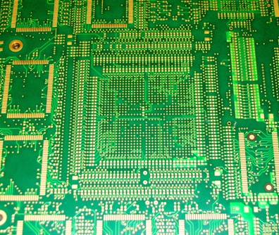
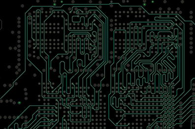
It can be in a standard form factor or in a custom shape. All boards have nowadays some things in common: they have a huge number of components, usually both sides and a high density of routing.
Most of the modern boards feature high-speed lines and high power requirements.
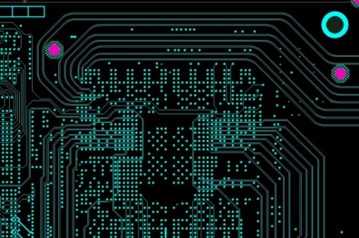
We do boards design for 10 years already. We accumulated a tremendous experience in dealing with tight space for placing thousands of components,
high power dissipation, high-speed differential pairs in the hundreds, DDR3 memory routing and high-speed base materials for the boards.
We also gained the experience to deal with tight schedules.
One aspect that our customers always highly appreciated while working with us is that we
analyze the schematics for inherent errors.
Never had happened that a schematic error escaped our experienced electronic engineers.
We use our expertise to offer the best layout solutions even when the constrains are set in the
schematic. Our customers often adopt our advise and include it in the specs. |